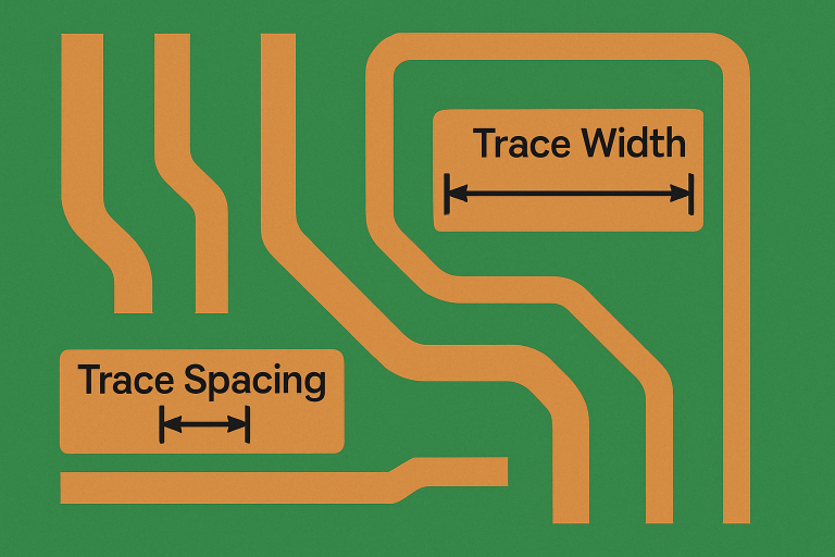
Understanding the Importance of Trace Width and Spacing
PCB design is crucial for modern electronic systems, with trace dimensions—specifically, width and spacing—significantly affecting reliability and performance. Errors can result in signal losses, noise, or circuit failures. Expertise in design ensures precision, leading to robust outcomes, while careful trace layout differentiates high-quality boards from those with EMI issues, excessive heating, or manufacturing complexities. For advanced design precision and professional PCB layout services, consider working with Allegro design Massachusetts. As electronics become smaller, faster, and more complex, understanding and optimizing these parameters is essential for anyone involved in electronics design and fabrication.
Collaborating with experienced PCB designers ensures that every trace, via, and layer is optimized for performance and manufacturability. Modern design tools and simulation software can help predict potential issues early, reducing costly revisions and production delays. Ultimately, investing in expert PCB design not only enhances product reliability but also supports faster time-to-market and long-term operational efficiency.
Factors Influencing Trace Width Selection
Choosing the appropriate trace width is much more than a matter of layout aesthetics. Several engineering demands contribute to this decision, each with implications for performance and longevity of the circuit.
- Current Carrying Capacity: The width of a PCB trace is directly related to the amount of current it can safely carry. Thin traces tend to heat up quickly when loaded, which can sometimes lead to board or component failure. Wider traces dissipate heat better, allowing them to handle greater currents. Following IPC-2221 standards, for example, a 1mm-wide trace at a standard copper thickness can generally handle 1A of current, while higher currents require a width of up to 5mm or the use of polygon pours.
- Signal Integrity: High-speed and high-frequency signals require special attention, particularly in terms of impedance matching. Transmission line effects become prominent at higher speeds, so trace width must often be tightly controlled. For standard digital signals, 50Ω characteristic impedance is common for single-ended traces, and 90Ω for differential pairs. Adjustments to stack-up and trace geometry—using microstrip or stripline methodologies—help meet these targets and maintain clean waveforms.
- Thermal Management: The trace width also impacts the temperature rise under load. Wider traces spread heat more efficiently, ensuring local hotspots don’t build up near sensitive components or connectors.
While computer-aided calculations and impedance control are now standard best practices, designers must also consider the board layer configuration as part of this process. With proper planning, potential hazards such as overheating and signal distortion are minimized, letting the layout deliver its full intended functionality.

Determining Optimal Trace Spacing
Trace spacing serves as your board’s first defense against crosstalk, arcing, and shorts. The relationship between adjacent copper paths isn’t just about fitting routes onto the board; it has a direct bearing on electrical safety, signal clarity, and compliance with both industry and manufacturer guidelines.
- Voltage Levels: The potential difference between traces dictates the required isolation distance. The IPC-2221 standard sets recommended minimums; for example, traces carrying up to 15V should be spaced at least 4 mils apart. Higher voltages require even more generous spacing to prevent arc-over or creepage impulses.
- Signal Frequency: Speeding signals tend to radiate electromagnetic energy, potentially inducing noise in neighboring lines. The “3W rule” (three times the trace width) is a helpful heuristic for suppressing crosstalk. By ensuring that traces with high-frequency signals are separated by at least three times their width, electromagnetic coupling can be significantly reduced.
- Manufacturing Constraints: Even the best theoretical layout is subject to real-world manufacturability limits. Each PCB house will specify a minimum trace spacing—often between 4 and 10 mils for standard processes—below which defects and yield issues multiply.
Even experienced engineers benefit from referencing the latest industry standards and updated manufacturing guides. This ensures no details are overlooked as device voltages, signal speeds, and board densities increase.
Implementing Design Tools and Calculators
High-quality CAD tools and online calculators streamline the process of optimizing both trace width and spacing. Design software such as Altium Designer, OrCAD, and the Saturn PCB Toolkit enables easy calculations for current, temperature rise, and impedance, saving hours of manual computation. These tools enable iterative adjustments for stack-up, copper thickness, and trace routing, ensuring the desired results before boards reach the fabrication stage.
Adhering to Industry Standards
Following standards like IPC-2221 isn’t just about technical correctness; it’s about designing for reliability, safety, and smooth manufacturing. IPC-2221 outlines broad recommendations across trace width, spacing, current, and voltage criteria, offering a trusted baseline for nearly every PCB application. Adhering to these proven guidelines streamlines communication with manufacturers and minimizes costly redesigns or errors during production.
Ultimately, industry standards serve to align design intent with what is physically possible and commercially viable. Compliance ensures consistent product quality, mitigates the risk of field failures, and increases compatibility across global supply chains. No design is complete until it fulfills these external benchmarks.
Conclusion
Optimizing trace widths and spacing is a crucial element in modern PCB design, underpinning every aspect, from power delivery to high-speed signal integrity. Through careful planning, use of up-to-date design tools, and strict adherence to industry standards, engineers ensure the reliability, efficiency, and manufacturability of their boards. These practices equip teams to meet the rising demands of today’s electronic applications, guaranteeing project success and long-term product lifecycle performance.
